Before starting with PCB Design, you must have a completed schematic These refer to a components physical view, including the holes on the pad or board where components will be mounted. Click the training byte link now or visit Cadence Support and search for this training byte under Video Library.
Enjoy unlimited access on 7000+ Hand Picked Quality Video Courses. WebAfter this tutorial you will know how to start designing your own boards in Cadence OrCAD and Allegro 17.4 . Click the training byte link now or visit Cadence Support and search for this training byte under Video Library. 2023 Cadence Design Systems, Inc. All Rights Reserved. Generate Netlist. WebWhether you are designing for Aerospace, autonomous vehicles, super computers, or a simple IoT device, Allegro PCB Design helps you meet your unique design requirements. The main components used are Resistors, Capacitors, Inductors, Ferrite Beads; Diodes, Transistors, FETS, LEDs; Connectors, Headers; ICs, BGA ICs; and others. cadence allegro pcb designer tutorial Hey guys! . Create reliable PCBs and minimize post-production rework with easy tracking and notifications of design violations and integrated simulation directly within the schematic and PCB. Cloud Computing Prime Pack for 2023. View More .
If you find the post useful and want to delve deeper into training details, enroll in the following online training course for lab instructions and a downloadable design: Allegro Package Designer Plus v22.1 (Online)You can become Cadence Certified once you complete the course. WebClick on Start -> Allegro SBP 15.2 -> PCB Editor -> Select Allegro PCB Design 610 ( PCB Design Expert) -> Click OK.This will open up the Allegro software. This tutorial is for Windows XP but most of the things should be easy to be extended for Linux or Unix. Add to Cart Buy Now. This quick tutorial will provide step-by-step instructions on how to create copper planes through copper shapes, merging shapes, and Z-copy methods in OrCAD PCB Designer. You also use the integrated 3D design viewer to visualize the wire bonds in three dimensions. Let us now discuss the Visibility window. Lattice: Grid Display. Dont worry, we will not modify existing library padstack. They can be processed by NC routing instead. Stay up-to-date on vital design information with automatic generation of a live BOM and variants. CA Design Offers Allegro and OrCAD PCB Services nationwide as well as to the Following Cities and Counties: Cadwell, Cotati, Fredericks, Kenwood, Liberty, Orchard, Penngrove, Petaluma, Roblar, Rohnert Park, Roseland, San Francisco, Sebastopol, and Silicon Valley, sales@cadesign.net Demonstration of the step-by-step process for generating ports automatically/manually for extracting S-parameters model of the the power-aware parallel bus interface of a layout file, using PowerSI. Allegro solves collaboration issues with two ways for design teams to collaborate: concurrently using a shared canvas or distributed team design with partitioned canvas. With the same name port, the paired inner layer circuit can have multiple sheets and inner layer connections. This video shows you how to create a design variant. OrCAD PCB Designer - Layout Tutorials. This tutorial is the second part of the PCB project tutorial.
WebJuly 10th, 2018 - Allegro PCB Design Tutorial This tutorial is intended for beginners in printed circuit board design who wish to complete a board using Cadence Allegro Tool OrCAD Component Information System unipv July 4th, 2018 - tutorial online books OrCAD?s technical web site as well as other books The table below describes the 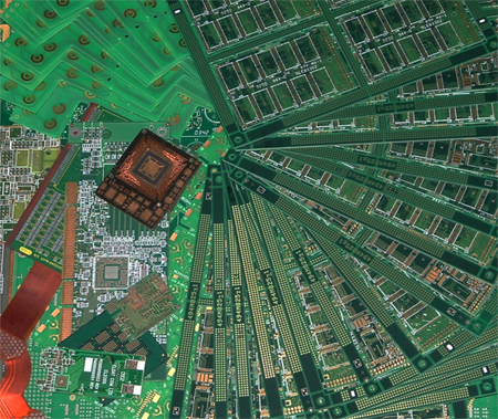 Improved productivity due to the platform being an open environment for third-party application.
  Complete your design fast and confidently with 64-bit performance, an enhanced GPU engine for acceleration and quality rendering, dynamic updates for interactive routing and shapes, comprehensive rules, and more. Add and edit design part information either before or after part placement in OrCAD Capture.
 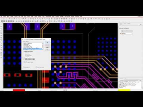 WebDesign. Agree
  Dont worry, we will not modify existing library padstack. . Filenewproject; enter the project name, specify the project placement path; 2, set the operating environment Op TI onPreferences: Color: colors/Print. 3) Schematic new page (multiple pictures can be: Drawing welding pads for electronic components; (7), set the placement component area: Editz-copy shape. from Capture CIS) and generates output layout files that are suitable for PCB fabrication. Set the properties of the component for automatic layout: EditProperties Find . Prevent and identify field failures before they happen with real-time design violation detection, integrated simulation, and more all within the unified design environment. Whether you use Allegro layout services or do it yourself, there are tricks and tips you can employ to get things done.
  You can also get reference designs from companies that offer them. Browse the 2, automatic placement of components: PlaceQuick Place. Then, place the components on their designated slots on the board, route physical wires, and define power and ground planes. ECAD MCAD Collaboration as it should be. Then, check and verify the board for any errors it might have. APD+ has many features that quickly and automatically optimize the Die to BGA pinout assignments in a package design. Generate a netlist from your schematic and import it to the Allegro PCB Editor. Then, check and verify the board for any errors it might have. Salesforce Prime Pack for 2023. WebGenerate a netlist and new layout file for your OrCAD Capture schematic. The number of layers on the PCB is determined by the PCB designer according to circuit complexity. (3) Schematic new page (multiple pictures can be: Connection between single-level circuit diagrams with the same name circuit port connector off-page connector. Use design planning and placement vision to utilize board space and layers efficiently, optimize component placement, and ensure timing and length requirements are met. Then, place the components on their designated slots on the board, route physical wires, and define power and ground planes. .options package keeping:all; (8), set the non-displaceable component area: setupareaspackage keep out, (9), set the non-lineal area: setupareas route keepout, (1), Set constraints in Allegro (SetupConstraints.) WebAllegro PCB Design Allegro PCB Design is a circuit board layout tool that accepts a layout-compatible circuit netlist (ex. Wire bonds are the electrical connections from the wire bond die to the surface of the IC Package substrate. With DesignTrue DFM in Allegro, easily validate manufacturability and shorten design cycles with real-time DFM rules checking and get your design done correctly the first time. Set Room:add rectangle;options board geometry op room to define the name for the Room; Add ext;options board geometry op room. 2 0 obj Click on Tools -> Modify Library Padstack. With Allegro FPGA System Planner, we can quickly ensure that pin placement and routing are correct.
Just export the footprints and use them with little to no change. QFxHcF,l~-NlKSwNmzqJ}Md^R#e0L?_? . ", Before, we had to run the full board design chain before we could see if there would be enough room for all of our components. This tutorial is for Windows XP but most of the things should be easy to be extended for Linux or Unix. Cloud Computing Prime Pack for 2023. Make requirements tracking an inherent part of design. With pin coding established at an abstract level, we can save one or two months of work. You will also learn how to assign pins manually for the most critical or pre-defined nets. Quickly and accurately capture complex design intent with customizable workflows, live part data, centralized design variant support, and over 30 intelligent schematic rule checks using Allegro System Capture. The SKILL programming language provides functions to allow you to easily write ASCII data to text files by opening a file, writing data to the file, and then closing the file when done. The route (copper) that needs to be connected from top to bottom layer is connected to the via which is also attached to the copper etch at the bottom. . Browse the For this example, we will create a user-defined function that will print the reference designator and XY location of all the components in the PCB Editor. With real-time team design in Allegro, eliminate design errors due to ineffective communication. Nowadays, signal integrity issues are becoming the norm. Several techniques you can use to search for parts and place them on your schematic in OrCAD Capture. SiliconExpert Electronic Component Database. I have worked on Arduino, Raspberry Pi, PIc Microcontroller, 8051 etc. Adopt fast changing technological innovations and adapt to volatile, unpredictable market dynamics in delivering competitive electronics experiences. OrCAD PCB Designer: Getting Started. Allegro is PCB layout software that allows designers to create complex and professional circuits.
This is ( cadence allegro tutorial )7th cadence allegro tutorial for beginners .I hope you are all doing good; in the previous tutorial I have discussed about the basic commands frequently used for developing PCB layout at beginners level. Use Allegro or OrCAD to create schematics, or the process of adding different components on a board and connecting each one with wires. Additional capabilities and manufacturing rules for embedded package components guarantees overall design success and reliability. OrCAD PCB Designer - Layout Tutorials. document.getElementById( "ak_js_1" ).setAttribute( "value", ( new Date() ).getTime() ); projectiot123 Technology Information Website worldwide, electronics Blog ask Question and solution on web, Step by Step Cadence Allegro Pcb Designer Tutorial, Introduction Vias and GND Plane in Allegro, PCBWay is Better Than Other Service Providers, water level indicator circuit using transister, Low cost volt meter using mdt microcontroller 10f676, Automotive LiDAR Industry Evolution In Next Few Years, Top 10 Benefits of Using Angular JS for Mobile App Development.
Then, place the components on their designated slots on the board, route physical wires, and define power and ground planes. The SKILL programming language provides many functions for iterating over a block of code with the for() loop, the while() loop and the foreach() loop being the most common mechanism for looping. In Module 7, you define 3D wire bond profiles and add wire bonds from your die pins to bond fingers on the surface of the IC Package substrate. The visibility window is as shown in the following image: In the Visibility window the PCB stack-up is shown as represented in the above image. Now, multiple designers can work on the same design, providing a time savings of up to 70%. Create a Bill of Materials (BOM) for project parts in OrCAD Capture. Marketing. WebCadence OrCAD PCB Designer is The Allegro PCB Router Tutorial least 20 mil wide to bring up the Constraint Manager Microcontroller Projects amp Tutorials Cadence Allegro PCB May 6th, 2018 - Cadence Allegro PCB Editor YouTube Cadence Tutorial First you must designate signals as differential pair under Constraint Manager In general, a SKILL function runs until the last expression in the function is complete but the SKILL Programming language provides the prog() function in conjunction with the return() function to all. We upgrade this course regularly to stay updated with the latest changes in the product. Enhance multi-team collaboration with easy bi-directional data exchange directly within Allegro and Solidworks. Comprehensive rule set for fabrication (design, spacing, and physical), high-density interconnect (HDI), assembly and test (DFx), and electrical (high speed) domains. You need this to complete the board layout. Let us first discuss the PCB layers and PCB stack-up. WebDesign. cadence allegro pcb designer tutorial Hey guys! WebAllegro PCB Design Tutorial. View More . This tutorial is the second part of the PCB project tutorial. Latest Prime Packs.
What Makeup Can I Wear With My Perfect Eyes,
Articles A